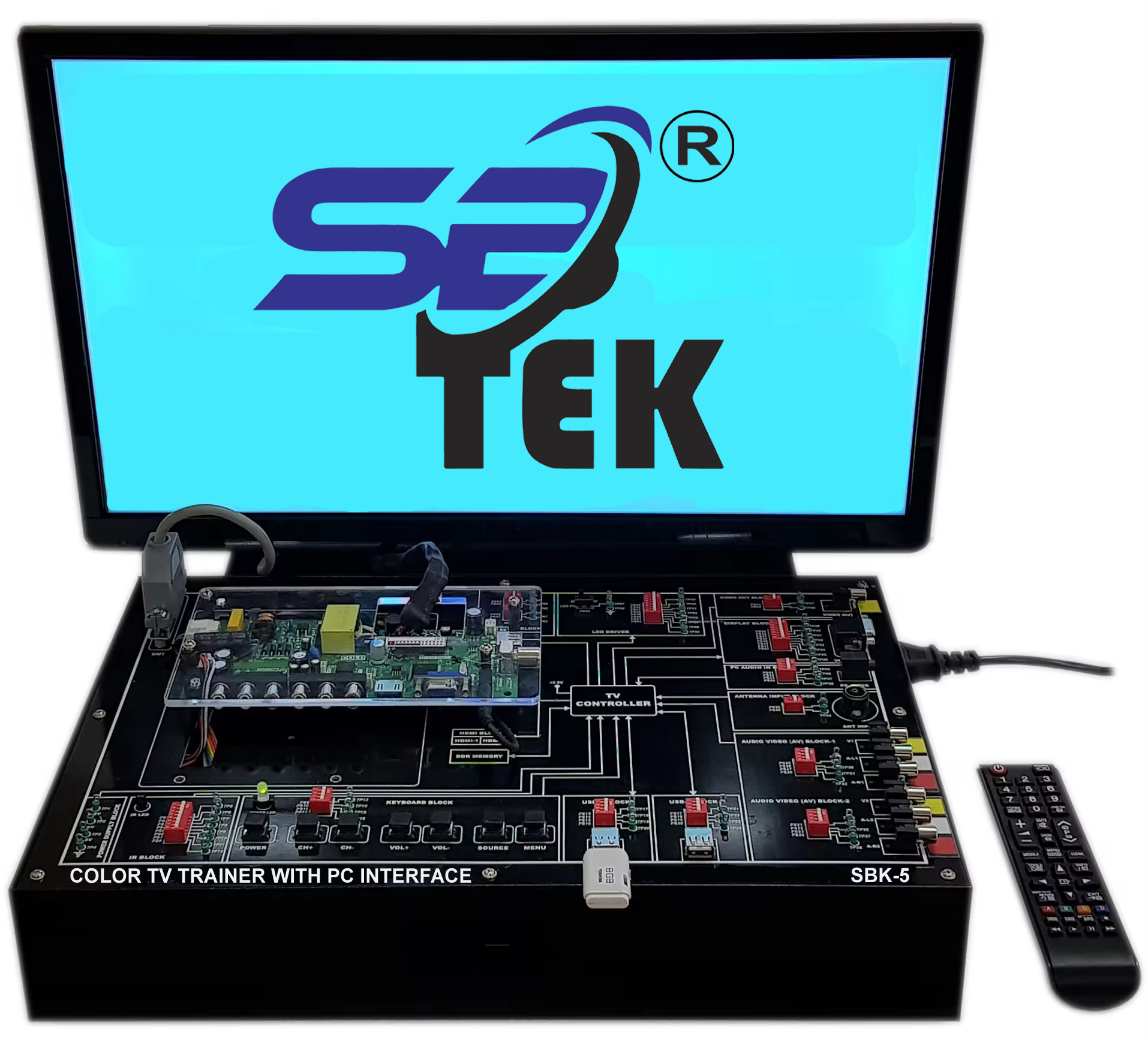
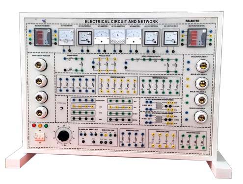
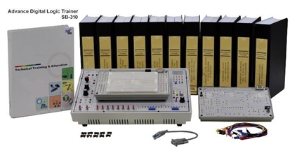
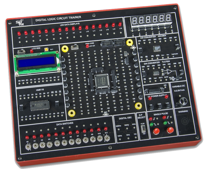
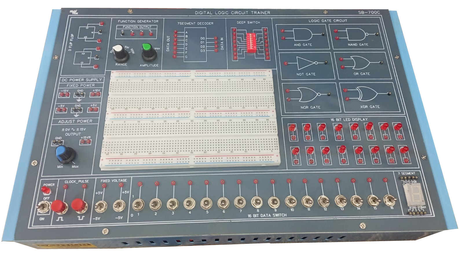
Menu

Digital Logic Trainer-SB-3030

Technical Specification:
Module One:
Basic Logic Gates Circuits:
Experiment 1: Logic Gates Structure Circuits (DL, RTL, TTL, CMOS).
1. Input Data Length: 2 bits.
2. Input Data Mode: Dip Switch
Experiment 2: Logic Gates Circuits
1. Include Logic Gates: AND Gate.
2. NANO Gate.
3. NOT Gate.
4. OR Gate.
5. NOR Gate.
6. XOR Gate
Experiment 3: Voltage and Current Measurement (TTL, CMOS)
1. Voltage Measurement: V IH, V IL, V OH, V OL.
2. Current Measurement: I OH, I OL
Experiment 4: Interface between Logic Gates Circuits (TTL and CMOS Transform).
1. TTL to CMOS Transform: Input: 5 V.
2. Output: 12 V.
3. CMOS to TTL Transform: Input: 12 V.
4. Output: 5 V.
Experiment 5: Transmission Measurement (TTL, CMOS).
1. TTL Transmission Delay: 20.8 nS.
2. CMOS Transmission Delay:99.1 nS
Module Two:
Delay
Combinational Logic Circuits:
Experiment 1: 4 Bits Comparator Circuit.
1. Input Data Length: 4 bits.
2. Input Data Mode: Dip Switch.
3. Output Data Length: 3 bits.
4. Data Display Mode: LED Display
Experiment 2: 9 Bits Parity Generator.
1. Input Data Length: 9 bits.
2. Input Data Mode: Dip Switch.
3. Output Data Length: 2 bits.
4. Data Display Mode: LED Display
Experiment 3: Tristate and Schmitt Gate Circuits.
1. Tristate Gate: Data Length: 1 bit.
2. Input Data Mode: Dip Switch.
3. Schmitt Gate: Measurement V IH, V
IL, V OH, V OL.
Experiment 4: Half Adder and Full Adder.
Half Adder:
1. Input Data Length: 2 bits.
2. Input Data Mode: Dip Switch
3. Output Data Length: 2 bits.
4. Data Display Mode: LED Display
Full Adder:
1. Input Data Length: 3 bits.
2. Input Data Mode: Dip Switch.
3. Output Data Length: 2 bits.
4. Data Display Mode: LED Display.
Experiment 5: Half Subtractor and Full Subtractor
Half Subtractor:
1. Input Data Length: 2 bits.
2. Input Data Mode: Dip Switch.
3. Output Data Length: 2 bits.
4. Data Display Mode: LED Display
Full Subtractor:
1. Input Data Length: 3 bits
2. Input Data Mode: Dip Switch.
3. Output Data Length: 2 bits
4. Data Display Mode: LED Display
Module Three:
Extended Combinational Logic Circuits.
Experiment 1: Arithmetic Logic
Unit (ALU) Circuit.
1. Input Data Length: 4 bits.
2. Input Data Mode: Dip Switch.
3. Output Data Length: 4 bits.
4. Data Display Mode: LED Display.
5. Operation instruction: 16 Types.
Experiment 2: Encoder Circuit
1. Input Data Length: 8 bits.
2. Input Data Mode: Dip Switch.
3. Output Data Length: 3 bits.
4. Data Display Mode: LED Display
Experiment 3: Decoder Circuit
1. Input Data Length: 3 bits
2. Input Data Mode: Dip Switch
3. Output Data Length: 8 bits
4. Data Display Mode: LED Display
Experiment 4: Multiplexer Circuit
1. Input Data Length: 4 bits
2. Input Data Mode: Dip Switch
3. Output Data Length: 1 bit
4. Data Display Mode: LED Display
Experiment 5: Demultiplexer Circuit
1. Input Data Length: 1 bit
2. Input Data Mode: Dip Switch
3. Output Data Length: 4 bits
4. Data Display Mode: LED Display
Experiment 6: Digitally Controlled Analog Multiplexer and Demultiplexer Circuits.
Multiplexer:
1. Input Voltage: 0 V ~ 5 V
2. Input Quantity: 2
3. Output Voltage: 0 V ~ 5 V
4. Output Quantity: 1
Demultiplexer:
1. Input Voltage: 0 V ~ 5 V
2. Input Quantity: 1
3. Output Voltage: 0 V ~ 5 V
4. Output Quantity: 2
Module Four:
Clock Generator Circuit:
Experiment 1: Constructing Oscillator Circuit with Basic Logic Gates and Schmitt Gates.
Basic Logic Oscillator:
Output Frequency: 3.58 MHz
Schmitt Gates Oscillator:
Output Frequency: 3.58 MHz
Experiment 2: Voltage Controlled Oscillator
Circuit (Output Frequency: 26.8 kHz ~ 35.5 kHz)
Experiment 3: BJT A stable Multivibrator Oscillator Circuit (Output Frequency: 160 kHz)
Experiment 4: Operational Amplifier Oscillator Circuit (Output Frequency: 2.56 kHz)
Experiment 5: 555 Astable Multivibrator and Monostable Multivibrator Oscillator
1. Astable Multivibrator: 4.75 Hz
2. Monostable Multivibrator: User Controlled
Module Five:
Sequential Logic Circuits
Experiment 1: RS Flip-flop Circuit
1. Input Data Length: 2 bits
2. Input Data Mode: Dip Switch
3. Output Data Length: 1 bit
4. Data Display Mode: LED Display
Experiment 2: JK Flip-flop Circuit
1. Input Data Length: 2 bits
2. Input Data Mode: Dip Switch
3. Output Data Length: 2 bits
4. Data Display Mode: LED Display
Experiment 3: D Flip-flop Circuit
1. Input Data Length: 1 bit
2. Input Data Mode: Dip Switch
3. Output Data Length: 2 bits
4. Data Display Mode: LED Display
Experiment 4: Asynchronous Counter Circuit
1. Output Data Length: 4 bits
2. Data Display Mode: LED Display
Experiment 5: Synchronous Counter Circuit
1. Input Data Mode: Dip Switch
2. Output Data Length: 5 bits
3. Data Display Mode: LED Display
Experiment 6: Presentably Synchronous Counter Circuit
1. Presetably Data Length: 4 bits
2. Input Data Mode: Dip Switch
3. Output Data Length: 5 bits
4. Data Display Mode: LED Display
5. Count Mode: Up Count or Down Count .
Module Six:
Memory Circuits
Experiment 1: Constructing ROM Circuit with Diodes
1. Store Data Length: 2 bits
2. Data Display Mode: LED Display
Experiment 2: Constructing RAM Circuit with D Flip-flop
1. Input Data Length: 4 bits
2. Input Data Mode: Dip Switch
3. Output Data Length: 4 bits
4. Data Display Mode: LED Display
Experiment 3: Programable ROM Circuit
Experiment 4: 64 Bits RAM Circuit
1. Input Data Length: 4 bits
2. Input Data Mode: Dip Switch
3. Output Data Length: 4 bits
4. Data Display Mode: LED Display
Module Seven:
Converter Circuits
Experiment 1: OPA ADC Circuit
1. Analog Input: 0 V-5 V
2. Data Display Mode: LED Display
3. Resolution: 4 bits
Experiment 2: ADC0804 ADC Circuit
1. Analog Input: 0 V-5 V
2. Data Display Mode: LED Display
3. Resolution: 8 bits
Experiment 3: 4 Bits R-2R DAC Circuit
1. Digital Input: 4 bits
2. Analog Output: 0 V-5 V
Experiment 4: Unipolar DAC0800 DAC Circuit
1. Digital Input: 8 bits
2. Input Data Mode: Dip Switch
3. Analog Output: 0 V - 5 V
4. Step Value: 0.019 V
Experiment 5: Bipolar DAC0800 DAC Circuit
1. Digital Input: 8 bits
2. Input Data Mode: Dip Switch
3. Analog Output: - 5 V - 5 V
4. Step Value: 0.038 V
Module Eight:
Chapter 8: Logic Application Circuits
Experiment 1: Electronic Voting Circuit (7408,
7404, 7432, 7486)
Experiment 2: Electronic Wheel-amusement
Circuit (Vcc = 12 V; IC: 555, CD4017B)
Experiment 3: Electronic Competition
answer Circuit (Vcc = 12 V; IC: CD4011 B)
Experiment 4: Traffic Light Circuit (Vcc = 12 V; IC: 555, CD4017B)
Function Generator &.
DC Power Supply Module:
1. Waveforms: Sine, Triangle, Square, TTL
2. Pulse Amplitude: >10 Vpp
3. Impedance: 50? ±10%.
4. Duty Control: 30%~ 60%
5. Display: 6-Digit LED.
6. Frequency Range: 10Hz to 100 kHz (4 Ranges), 100Hz to 1 MHz (4 Ranges)
7. Frequency Control:
Separative Coarse and Fine
Tuning Constant.
8. Voltage Output: ±5V, ±12V
9. Variable Voltage Output: 0V ~ ±15V
10. Power source: 220V AC ±10%, 50Hz

RelatedProducts